Hardware & PCB Engineering

PCB Design Services
from Schematic to Production Hardware

We deliver hardware and PCB design services for embedded products, connected devices, and electronic equipment with schematic capture, multilayer PCB layout, signal integrity analysis, prototype validation, DFM review, and production handover.

Schematic Design Multilayer PCB Signal Integrity DFM / EMC Prototyping
Discuss Your PCB Project Our Services
Hardware and PCB design for embedded electronics
1-8+Layer PCBs
DFMReady
FullCycle
1-8+
Layer PCBs
Mixed
Signal Expertise
EMI / EMC
Pre-Compliance
4+
EDA Platforms

What We Offer

Full Cycle Hardware
Engineering Services

We cover the full hardware design cycle in one place, from schematic capture and multilayer PCB layout to validation, manufacturability review, and production handover for embedded systems, IoT devices, industrial electronics, and customer-facing products.
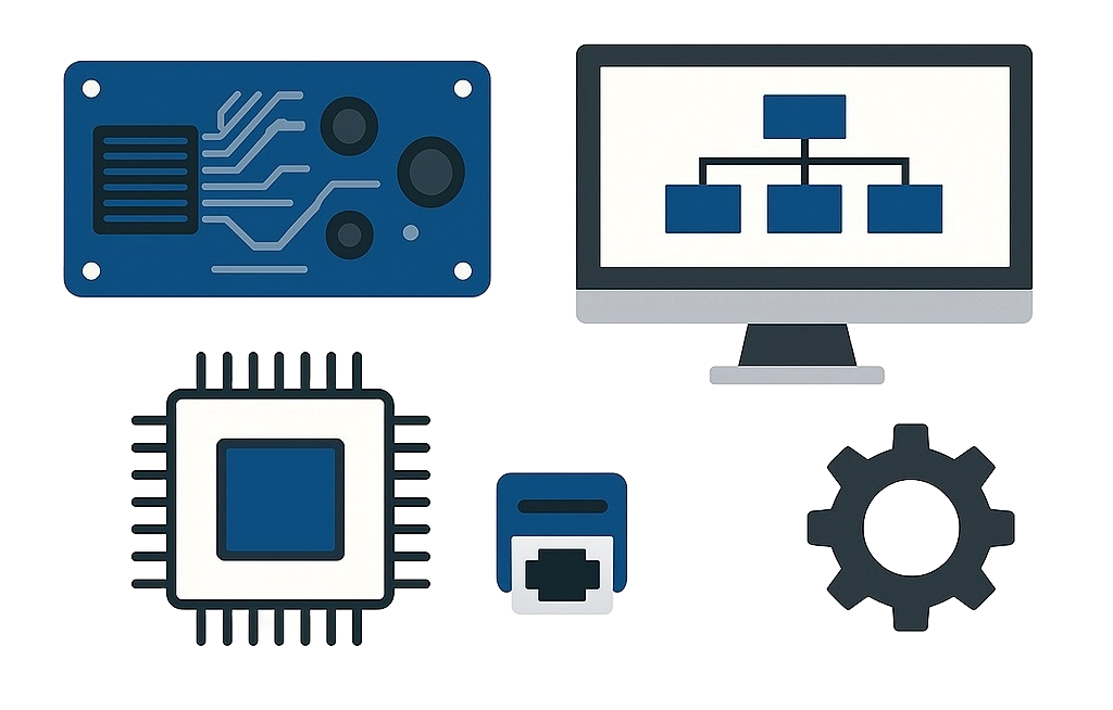
Schematic & Layout Signal Integrity Thermal Analysis EMI / EMC Production Docs
Hardware design overview
Concept & architecture

Schematic Design

We shape the electrical architecture before layout starts, balancing performance, power, cost, and manufacturability from day one.

  • Feasibility review, block diagrams, and proof-of-concept planning
  • Component selection, power trees, interfaces, and protection circuitry
  • Peer-reviewed schematic capture for analog, digital, and mixed-signal boards
Power architecture BOM aware
Board design

PCB Layout & Routing

From compact control boards to dense multilayer products, we route for performance, assembly yield, and mechanical fit together.

  • Single-sided, double-sided, rigid, and multilayer PCB layouts
  • Controlled impedance, differential pairs, via strategy, and stackup planning
  • Layout optimization for space, thermal behavior, and DFM-ready fabrication output
1-8+ layers Gerber ready
Analysis & robustness

Signal, Power & Thermal Integrity

We reduce respins by validating how the board behaves electrically and thermally before it becomes a manufacturing problem.

  • Pre and post-layout signal and power integrity checks
  • Analog, high-speed digital, and mixed-signal noise isolation strategies
  • Thermal analysis, eye diagrams, and PDN behavior review for critical nets
Mixed signal Thermal review
Validation loop

Prototyping & Testing

Prototype boards are not just assembled and powered on. We use structured bring-up, test evidence, and refinement cycles to stabilize the design.

  • Board bring-up, electrical validation, and automated jig planning
  • Functional, safety, and environmental test coverage where required
  • Iterative refinement across prototype spins until the hardware is production confident
Bring-up logs Test evidence
Manufacturing confidence

DFM / DFT & EMC Compliance

We review the board for manufacturability, test access, and EMI risk early so certification and production do not become late surprises.

  • Design-for-manufacturing and design-for-test reviews with corrective guidance
  • EMI and EMC pre-compliance checks, shielding strategy, and layout cleanup
  • Certification support aligned to CE, FCC, UL, and project-specific targets
EMI aware Certification support
Production handover

Production Documentation

Your manufacturing partner receives a complete, organized package instead of scattered files and missing assumptions.

  • Schematic sources, Gerbers, drill files, BOMs, and assembly drawings
  • 3D models, test instructions, electrical reports, and CM support notes
  • Optional production test software and fixture guidance for line validation
CM package IP handover

How We Work

Full-Cycle Development Process

From early requirements to production handover, every stage is visible, reviewable, and structured around reducing downstream risk.

01
Consultation & Feasibility

Product goals, interfaces, cost constraints, and technical risks mapped up front.

02
R&D & Concept Design

Architecture studies, part research, POC planning, and practical tradeoff decisions.

03
Schematic Design

Electrical capture, power tree definition, and design reviews before routing begins.

04
PCB Layout & Analysis

Routing, signal and thermal checks, and DFM clean-up for fabrication readiness.

05
Prototype & Verification

Bring-up, debugging, electrical testing, and spin refinement where needed.

Production Handover

Final manufacturing files, test support material, and release documentation delivered.

PCB Capabilities

Design Capabilities & Specializations

From high-speed digital platforms to precision analog and RF boards, we support the specialist engineering depth needed to move complex hardware into production with confidence.

01
High-Speed Digital

Multi-core processor and module-based designs with PCIe, SATA, USB, Ethernet, camera, and display interfaces routed for signal quality.

02
Analog & Mixed-Signal

ADC and DAC front ends, op-amp chains, sensor interfaces, power electronics, and noise-aware grounding for reliable measurement and control.

03
RF & Wireless

WiFi, Bluetooth, GSM, 4G, GPS, antenna routing, shielding strategy, and pre-compliance considerations for connected products.

04
EDA Toolchain

Altium Designer, KiCad, Eagle, OrCAD and Allegro, DipTrace, LTspice, and MATLAB for design, simulation, and release packaging.

Hardware Domains

Hardware Domains We Serve

These are the product domains we actively support with hardware and PCB engineering, where reliability, compliance, and maintainability matter most.

IoT Devices

Sensors, gateways, asset trackers

Industrial Automation

Controllers, panels, PLC-adjacent systems

Medical Devices

Diagnostics, monitors, wearables

Automotive / EV

Telematics, BMS, control units

Aerospace & Defense

Rugged electronics and avionics support

Energy & Power

Inverters, smart meters, control boards

Analytical Instruments

Lab systems and precision hardware

Consumer Electronics

Wearables and connected smart products

Deliverables

What You Receive From Us

Our handover package keeps manufacturing, testing, and ownership details together so your internal team or production partner can move forward without missing files or assumptions.


Schematic & PCB Source FilesNative Altium, KiCad, Eagle, or OrCAD project files with reusable libraries and revision-friendly source organization.
Gerber & Fabrication FilesManufacturing outputs with drill data, layer stackup, impedance notes, and fabrication instructions ready for your board house.
Bill of MaterialsManufacturer part numbers, approved alternates, sourcing guidance, and practical cost visibility for procurement teams.
3D Models & Assembly DrawingsSTEP models, assembly references, connector orientation notes, and integration details for enclosure and manufacturing teams.
Test & Verification ReportsBring-up notes, functional test evidence, electrical validation records, and key observations from prototype refinement cycles.
DFM / EMC Review PackageManufacturability observations, test-access recommendations, EMI mitigation notes, and pre-compliance support records.
Production Test SoftwareWhere required, fixture-side scripts and automated test logic to streamline validation on the production line.
Ownership & Handover SupportClear IP transfer, manufacturing coordination support, and documentation your internal team can maintain independently.

EDA Tools & Tech Stack

We support the platforms most hardware teams already use for design, simulation, and board bring-up.

Turn your Idea Into Reality Today

Discuss Your PCB Project